Surface Mount technology (SMT) is lower cost, much smaller and better pin density than it’s through-hole predecessor. It is intended to be mass produced on robotic assembly line who are rated on thousands of chips per hour of through put. A manufacture can build a thousand boards in a few days; however, it is hard to get one board built. We need to build boards and may need to iterate half a dozen times before it is turned over to the manufacture. There are companies that do assembly of small quantities of boards but they are quite expensive.
There are some great chips that only come in surface mount that is inaccessible to most hobbyist because they are surface mount. Sparkfun sells some break out boards (BOB) that allow the hobbyist to use standard through hole technology to access surface mount chips. Boards like mbed and arduino bring out the pins of a surface mount part so that they can be easily soldered to.
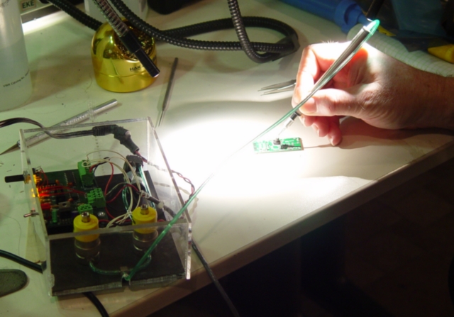
With the right equipment, it isn’t that difficult to assemble your own surface mount boards. In a past blog I describe a soldering station with Metcal soldering iron, Stereo Microscope, hot plate, IR temperature sensor, tweezers, etc.
I use solder paste with stencil and hot plate to do home made boards. I limit the SMT parts on one side of the board only. Through hole parts can be either side. Most of my passive parts are 0603 or larger. Smaller passives are doable just harder to manage. I do not use ball grid array (BGA), leadless packages (QFNs, DFNs) and for leaded quad flat pack I try to keep the pitch 0.8mm or larger. LQFPs that have 0.5mm pitch are completely doable although likely going to need rework with the solder wick and soldering iron. The process needs to be done in a fairly short time of hours so preparation is important.
Equipment
Hot Plate – I’d avoid toaster ovens, they are too awkward to get boards in and out of.
Stereo Microscope and good light source – make it look big when it isn’t
Good set of tweezers, xacto knife and a vacuum pick up wand – tweezers are good for placing small parts, knife for cutting paper tape strips and vacuum pick up wand is for placing the larger parts.
Solder paste – I use Kester solder paste made for stencil printing. You will need to know what RoHS requirements you need to work with to choose the solder paste. I keep my solder paste refrigerated. Kester specs the lifetime to 6 months. I usually can get a few years out of one can for this kind of work.
Alcohol and paper towels (for paste cleanup), squeegee (I use a plastic card), tape, solder wick (for rework), Popsicle sticks.
Make the stencil
The stencil is used to keep the paste on just the SMT pads. You can use the metal stencil although they are expensive they can be used many times. Another is to use one time use only stencils that are cut on a laser engraver. If you don’t have a laser engraver, usually someone who engraves name badges, signs etc has one. We have been using one time use only paper stencils. The paper we had the most success were low fiber high clay content such as used in high quality magazines with a lot of color photography.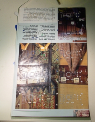 Yes, Playboy works quite well and it’s not just for the articles. The engraver doesn’t smolder when cutting as much as it does with regular paper and makes clean cuts.
When doing paper stencil, you should shrink the paste mask globally to accommodate laser width and burning. This is done by going into Design -> Rules…. and under Mask select Paste Mask Expansion. Set the paste mask expansion to -2mil to -4mil and apply.
To get a stencil file for an engraver, generate a DXF file. For early Altium designer, go into your PCB design and create the gerbers. This will generate a Altium CAM file. Select the CAM file and in the file menu select export. DXF will be an option. A popup will show with all the gerbers highlighted. Unselect all except select the top paste file (gtp) and the border outline (gm1 on mine). Set output control to zero width and click save. Another window will come up asking where it should be saved but the file name will always be cam.dxf. For later versions of Altium Designer open the PCB file, turn only the top paste and board outline layers. Do a save as, and select Export AutoCAD File (*.dwg, *.dxf). You will need to change the name to DXF file type. A dialog box will pop up and select AutoCAD Version (make sure the engraver can read this version of DXF file, some can’t read the latest), export as primitives is selected, Primitives to export with zero line widths is selected all and Layers is selected as “Currently Visible 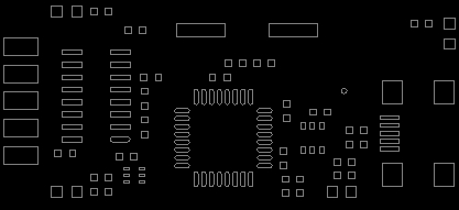 Layers”. Select OK. You should have something that looks like this
Preparation
Make sure you have all the parts for the build. I would suggest a quick electrical check of the board with a multimeter.
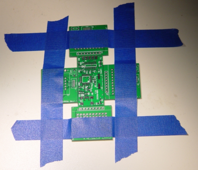 I use similar width small spare boards and use painters tape to attach them to a desk. The only thing important is that the boards are the same height as the board being assembled.
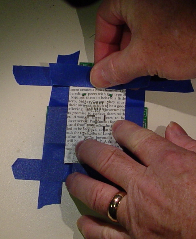
Next, put the paper stencil with tape on the edge that you will start pulling the paste down. Before sticking the tape down, line up the holes until everything showing through the stencil holes is shiny. You shouldn’t see any green just pads.
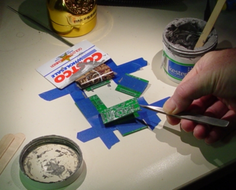
With a Popsicle stick, put a line of paste along the tape holding the stencil. It is better to have a little more than to little. The line should be as wide as the board, so that when it is drawn it will cover the whole board.
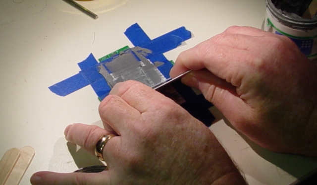
Put a firm pressure on a plastic card, pull the paste from the top of the board to the base with one slow even pull. This has to be done in one stroke. Do not go over it again if you missed any. Do not push the other direction. If there isn’t a clean pattern of paste or sections missed, remove the paste with alcohol, use a new stencil (if paper) and redo it.
Once the paste has been spread, gently pull back the stencil, cut the tape to release holding boards to carefully release the board. Be careful not to touch any of the stenciled pads nor smear the board. The stencil paste should be put back into refrigerator.
The board is now ready to be placed. All through hole parts will be placed after the SMT parts have been soldered. Start with the smaller passive parts and do the largest parts last. Go from the BOM and assembly drawing.
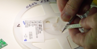
Parts can come on reels, tape cut from reels, lose parts or in tubes. The tape holds the part between a plastic or cardboard backing and a thin plastic tape. Peal back the plastic tape from the backing starting it with a sharp xacto knife. The section of tape that is used up can be cut off and disposed of.
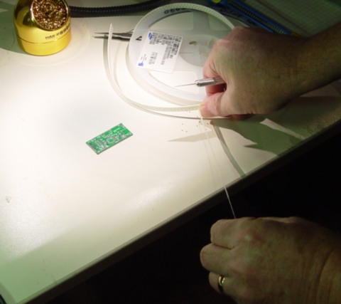 If it is cut tape make sure once the parts are pulled off that the tape that the cut tape is put back into the identifying bag. Parts rarely have markings that identify the part.
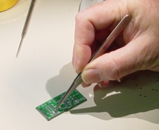
Passives and small parts can be on with tweezers under the microscope. Be careful not to touch the board nor nudge neighboring parts when placing a part. The parts are very light and it takes a very light touch to move them onto the paste. They do not have to be perfectly aligned. When the solder melts, the part will move into place from capillary action of the molten solder.
Larger parts may need a vacuum part pick up tool. Low cost hand operated one’s work as well as pump versions. The device to the left is one that I made for this application. It has a small rubber tip that holds a vacuum to pick up the part, it releases the vacuum to place the part.
Get the hot plate to a stable temperature next. Leaded solder liquefies at 183° C. It should never go higher that 225° C. Lead free solder liquefies at 217° C and should go no higher than 260° C. You can use an IR thermometer to monitor the temperature of the plate.
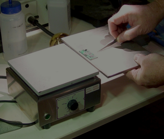
Once all the surface mount parts are placed, slide the board on a chunk of stainless steel. Then nudge the part over to the hot plate. Stabilize it at liquefied temperature and allow it to raise for 20 to 60 seconds or reaching peak temperature. Before it hits peak (-5° C below peak) turn the temperature down.
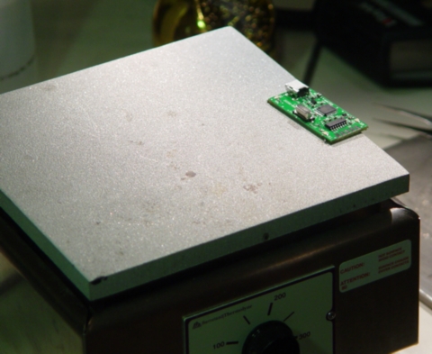 You should see the solder melt and the parts will move slightly as the solder liquifies. Carefully slide the PCB off of the hot plate onto the steel plate and let it cool.
Once it cools, examine the board for parts that shifted off of pads, for solder bridges, blobs of solder, and any other defect. With very fine pitch parts, it may require removing solder bridges using solder wick. I use a broad tip on the soldering iron with a narrow wick. Be careful not to pull the wick as this can damage the fragile pins.
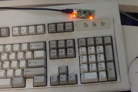
The board used in these pictures was a USB to serial converter using the AT90USB162 processor and the LUFA stack. It required no rework after reflow and I was able to program the application and it worked.
